Wikipedia links
Bode diagrams
--- http://en.wikipedia.org/wiki/Bode_plot
Hendrik
Bode --- http://en.wikipedia.org/wiki/Hendrik_Wade_Bode
History of the op amp (from Analog Devices)
http://www.kelm.ftn.uns.ac.rs/literatura/mpi/pdf/Op%20Amp%20Applications%20Handbook.pdf
Asymptotic (straight
line) Bode Diagrams
How to Find Stability from Bode
Criteria
for output with no input -- an oscillator
Bode slope reveals circuit
phase
Phase Margin & Transient
Response
Estimating Phase
Margin from Bode Diagram
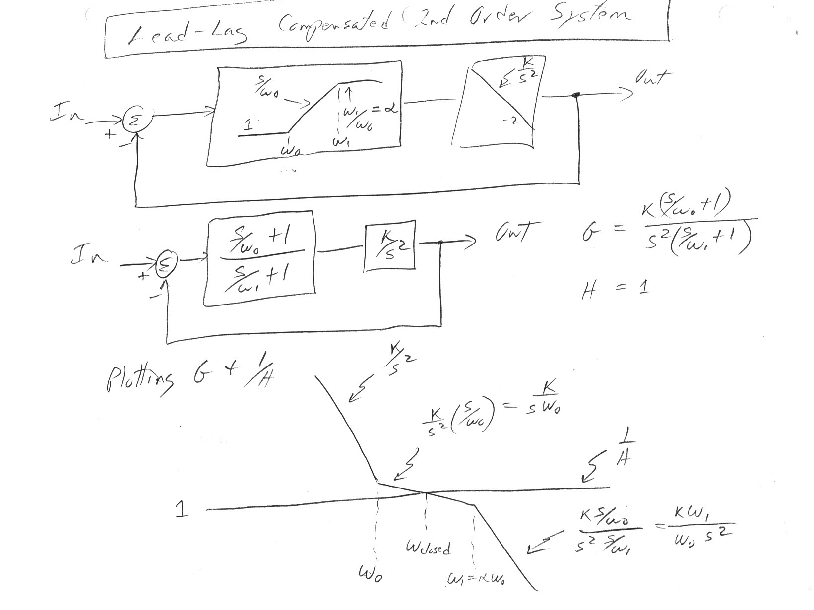
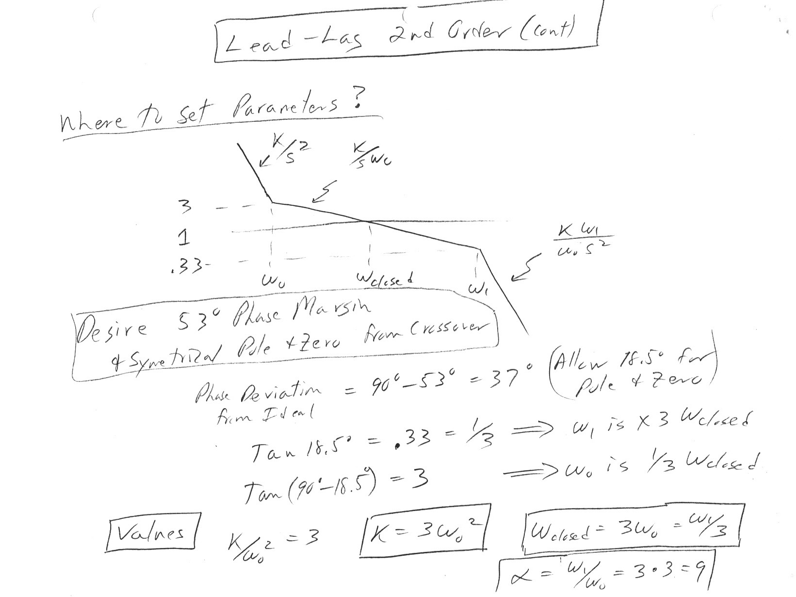
Lead-lag magnitude and phase curves
Lead-lag compensated
2nd order system
Op Amp Stability Analysis
Vintage Bode Diagram
reference handbook
Getting the Most from Bode Diagrams
Bode diagrams
are very powerful for the design and analysis of feedback control system,
much more useful than you would guess from the bare bones explanation of
bode diagrams in most textbooks. In 2001 while still working I wrote up
a detailed bode diagram tutorial reflecting what I had learned and used
in 40 years of designing motor control systems. My message here is once
Bode diagrams are well understood with a little practice you will be able
to estimate in your head how the the placement of poles and zeros affects
phase margin. This makes compensating a new loop easy, you can just sketch
out options for pole/zero placement.
Much of this information I had originally learned from a little softcover book (long out of print) on bode diagrams from one of the early op amp companies (Burr Brown?) published in the 60s or early 70s. I recently rediscovered my bode diagram viewgraphs in my files. I think it is a nice piece of work, so I am putting it online for engineers and engineering students.
Asymptotic
(straight line) Bode Diagrams
A circuit
analysis program can plot the exact magnitude and phase response of a circuit
or control loop. While this can be useful to check a final design, to verify
that it has the required BW (bandwidth) and phase margin, it is not
the
tool you want to design the control loop. The reason is that for a circuit
of any complexity the real magnitude and phase responses will be too soft,
too hard to adjust. For design purposes you want a straight line approximation
to the transfer function so you can 'see' where the poles and zeros of
the forward path (G) and the feedback path (H) are located. These frequency
breaks and the gains will need to be adjusted to get the desired control
loop response. Credit for the 'straight line asymptotic' trick to make
loop easy goes to Hendrik Bode in 1938.
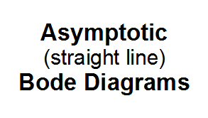
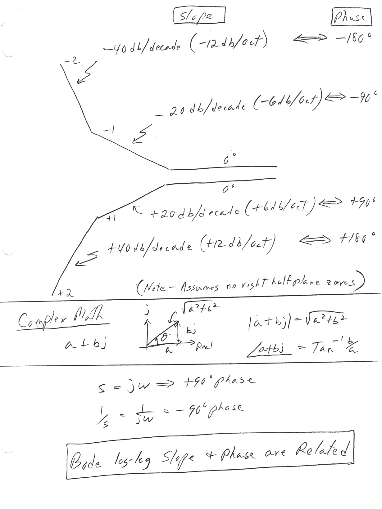
The goal is to derive a straight line (asymptotic) approximation of the transfer function of your circuit. Each straight segment will be a plot of a dominant term of the transfer function over the frequency range where it is dominant. This will be a log-log plot of magnitude vs frequency so terms incorporating frequency (s^2, s, s^0, s^-1, s^-2, etc) will plot as straight lines with different slopes, the slope set by the exponent of 's'. In such a plot the frequency of the poles and zeros are easy to see as they sit at the intersections of the straight line segments.
What we want is an equation of the transfer function with the poles and zero visable. Often it can be written by inspection, but it may take some playing around to get a single transfer function if a block has several circuits in series expecially if the some of the poles or zeros are not too separated. Multiply out the individual transfer functions to get a single transfer function with polynomials in terms of power of 's' in the numerator and the denominator.
Key idea
The key idea is
to separately take the numerator and denominator polynominals and assume
that over some frequency range a single term in the equation is
dominant. Just retain that term over that frequency range and drop the
others. Plot it up and label each straight line segment with its simplified
transfer function (as shown below). The intersections of the straight line
segment will give the poles and zero in terms of the constants in the equation.
Don't worry about the gain at this point, it will be adjusted during the
design process.
---------------------------------------------------------------------------------------------------------------------------------------------------------------------------------------------------------
Breaking out the electronic integrator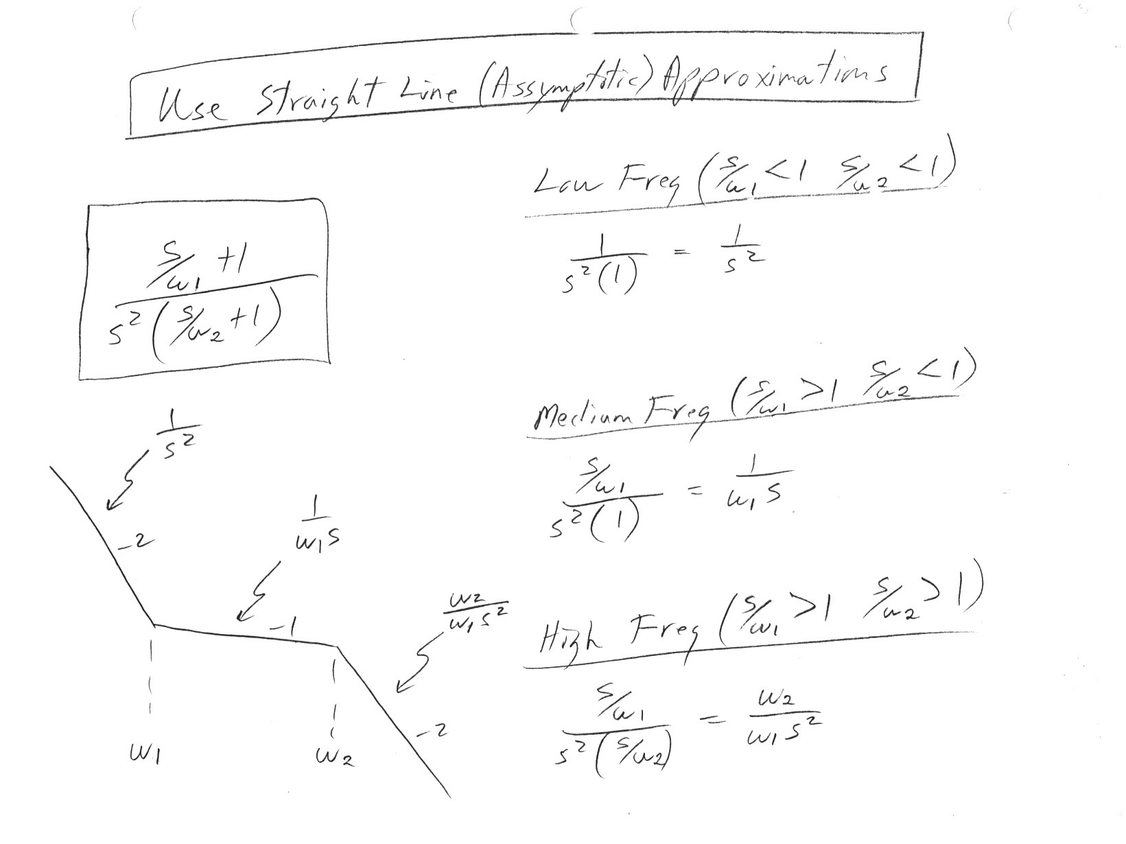
..
Crossover frequency
Hence typically
the gain is adjusted so the loop crossover is between w1 and w2. That is
the electronic integrator break zero out is set below the loop crossover
and the pole at w2 is set above the loop crossover. Ideally crossover would
be set at the geometric mean of w1 and w2 [sqrt{w1^2 + w2^2}] because this
frequency has the best phase margin, i.e. the lowest phase lag around the
loop.
Noise filter pole
While a system with
just an electronic integrator may be stable and tight, its real world performance
is likely to be poor due to high frequency noise. Almost all real control
systems need some noise filtering. For a motor to rotate smoothly and to
minimize heating from high frequency noise currents a low pass 'noise filter'
is usually required to attenuate noise spikes and other high frequency
electrical noise that always exists. Adding a first order low pass 'noise
filter' at w2 creates the first order pole in the bode diagram above at
w2. A noise filter would normally be set to 'break in' after the loop has
crossed over.
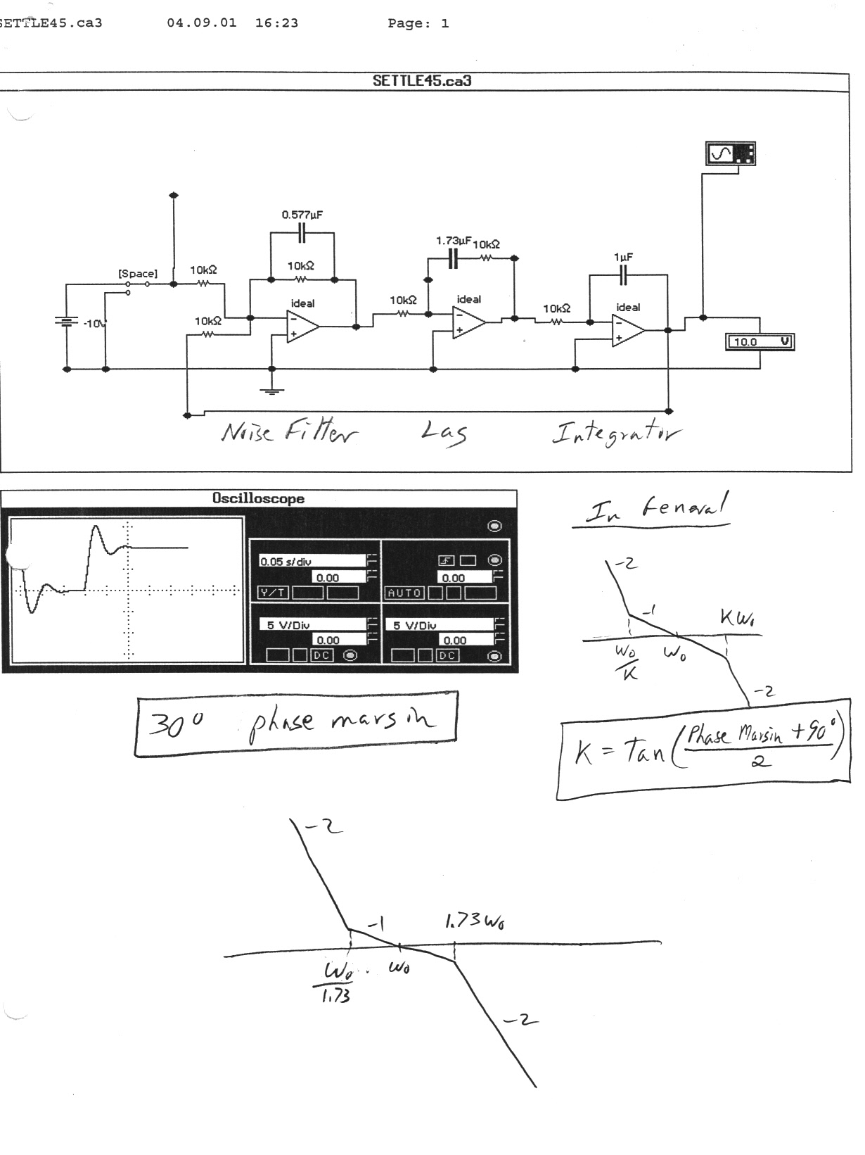
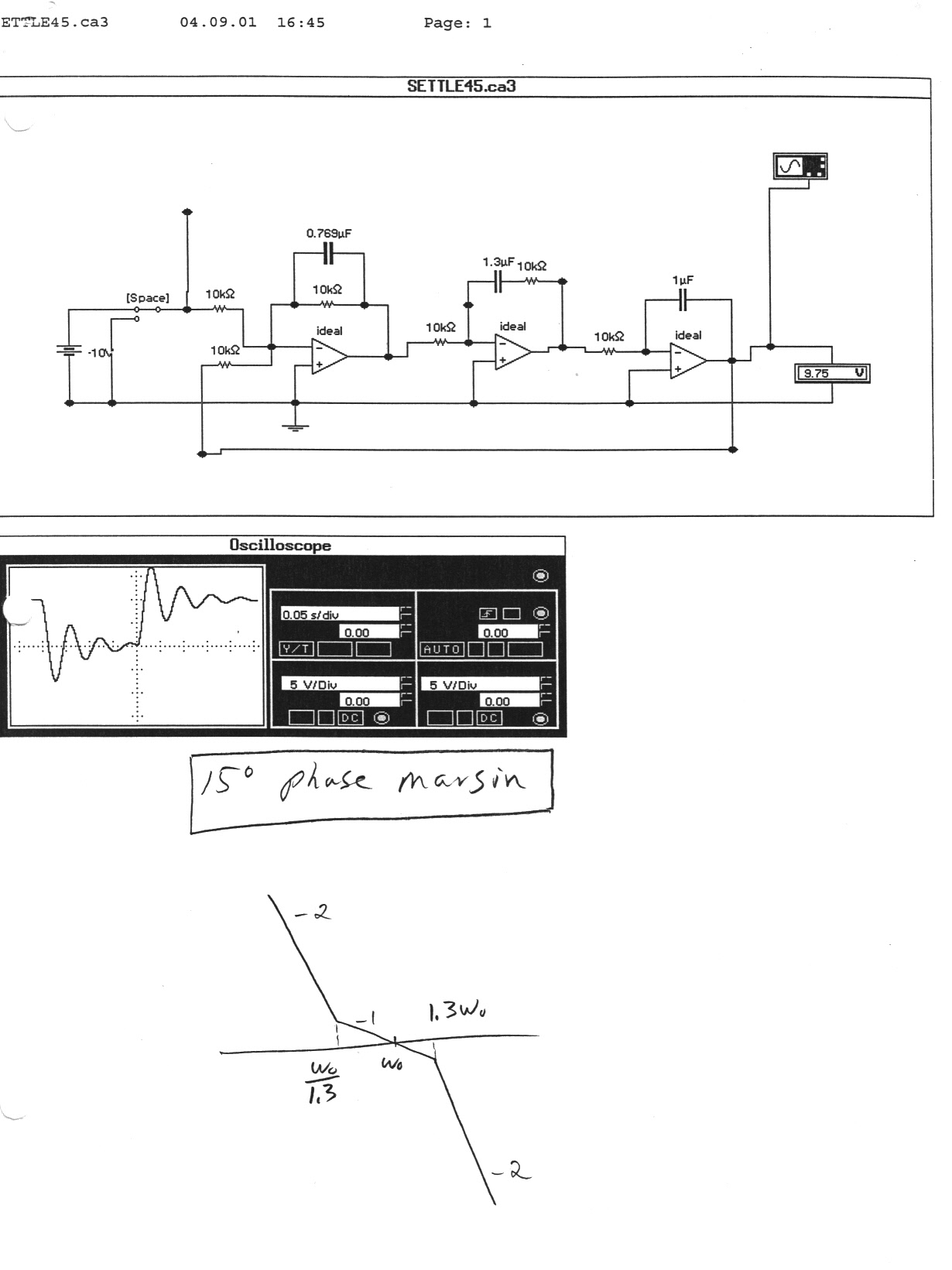
There you have it. A high performance control loop for a 1/s inertia load is tightened by an electronic integrator that is broken out below crossover, and noise is attenuated by a noise filter that breaks in above crossover. Even though the lag of the noise filter comes in strongly above its pole at the crossover frequency some of its phase lag is still 'visible'. While the breakout of the electronic integrator zero is positioned below the crossover frequency, it is not fully broken out at crossover, so it can be thought of as creating (in effect) some phase lag that is 'visible' at crossover. Hence both the (noise filter) pole and the (integrator break out) zero reduce phase margin at crossover. The closer they are to crossover the lower the phase margin, but the higher the loop performance.
For example
if a slightly underdamped transient response is acceptable, then a 45 phase
margin will do the job. The loop gain would be set so that the loop crosses
over in -1 slope region approximately midway between the zero and pole
(ideally at the geometric mean), where a -1 (or 1/w) slope on a bode diagram
implies (ideally) 90 phase lag (see below). For 45 degree phase margin
the sum of lags from the zero and pole can contribute an additional 45
degrees lag. If positioned symmetrically around crossover, this is 22.5
degrees each. Knowing their phase contributions at crossover allows the
frequency of the pole and zero to be calculated. Since [tan(22.5 degrees)
= .414 and 1/tan(22.5 degrees) = 2.41], the integrator breakout zero located
at x.414 of loop crossover and the noise filter pole located at x2.41 loop
crossover will give the desired loop stability with a 45 degree phase margin.
---------------------------------------------------------------------------------------------------------------------------------------------------------------------------------------------------------
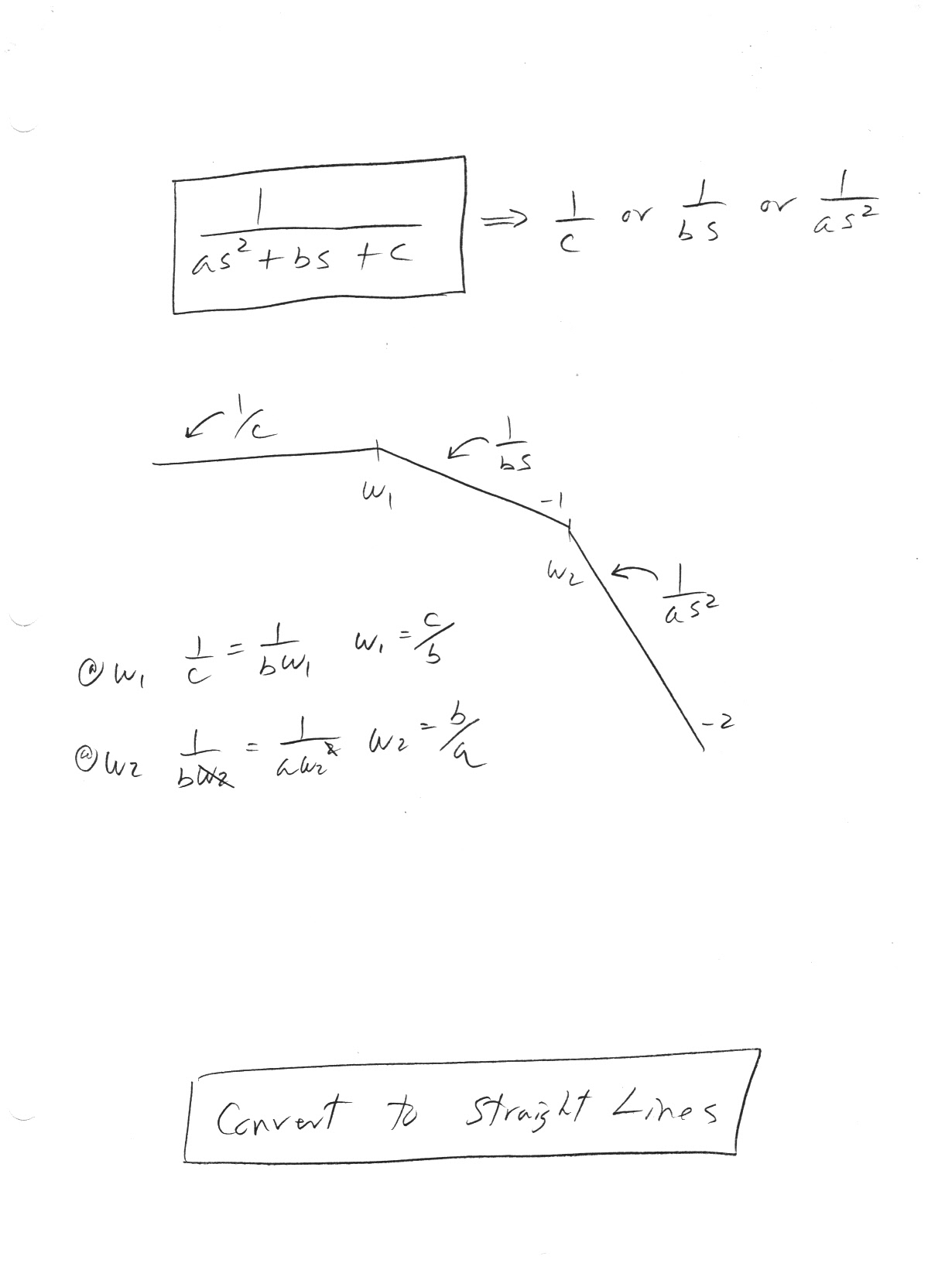
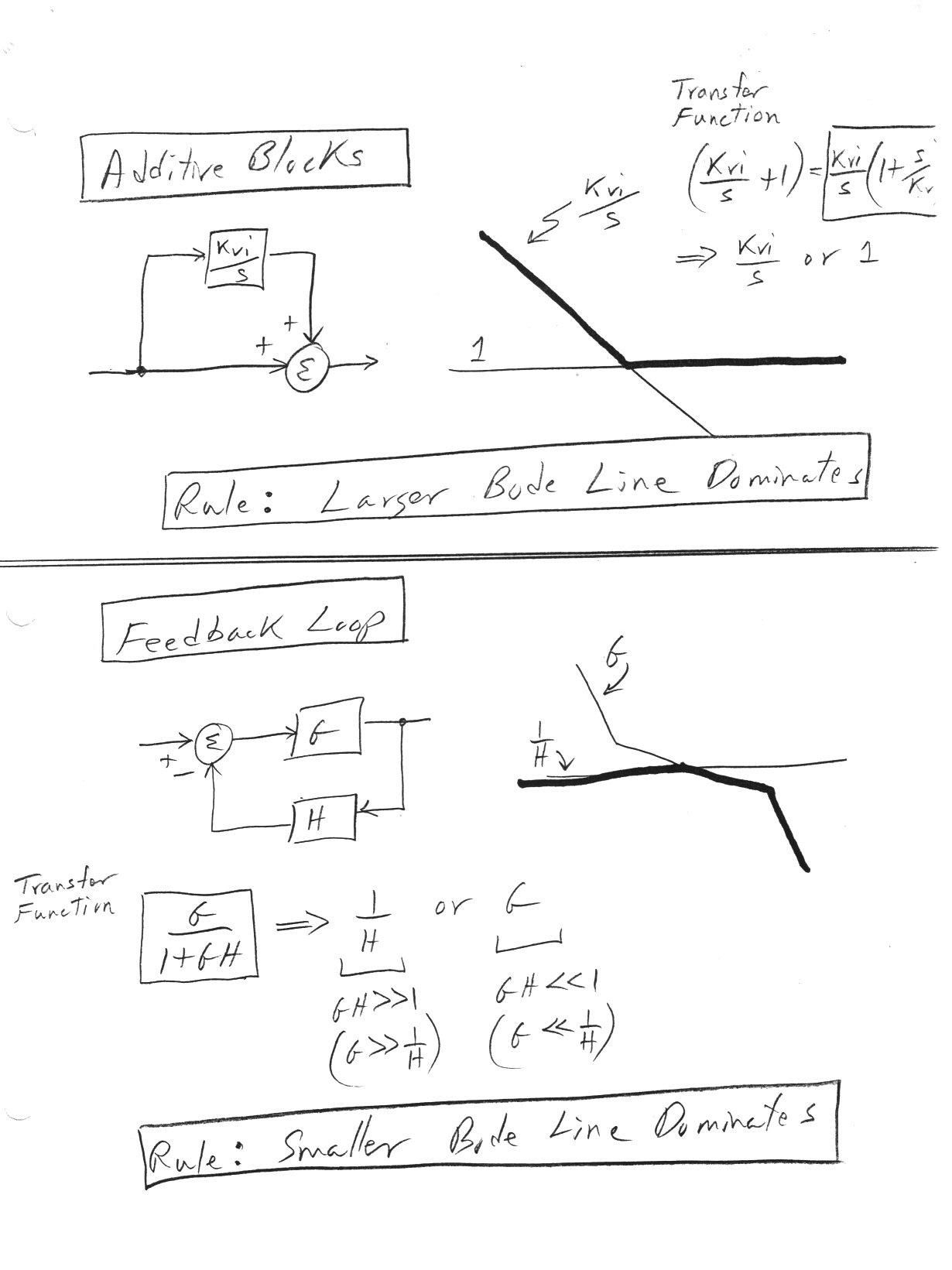
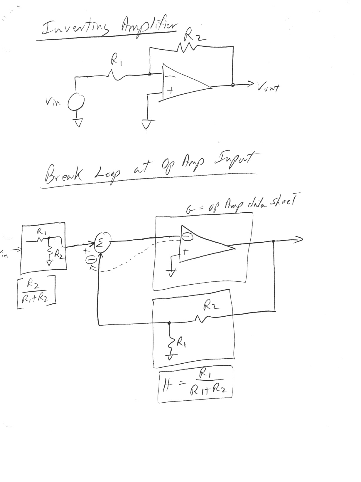
Combining blocks
The straight
line asymptote of usual (negative) feedback configuration [G forward path
and H feedback path] is found by assuming that the closed loop (in/out)
response follows the inverse of the feedback path straight line asymptote
(1/H) when when [G > (1/H)] and follows the forward path straight line
assumptote when [G < (1/H)]. This translates into plotting the 1/H and
G straight line asymptotes and the smaller dominates. If the paths
are additive, then the larger dominates.
---------------------------------------------------------------------------------------------------------------------------------------------------------------------------------------------------------
Here's a worked out example.
---------------------------------------------------------------------------------------------------------------------------------------------------------------------------------------------------------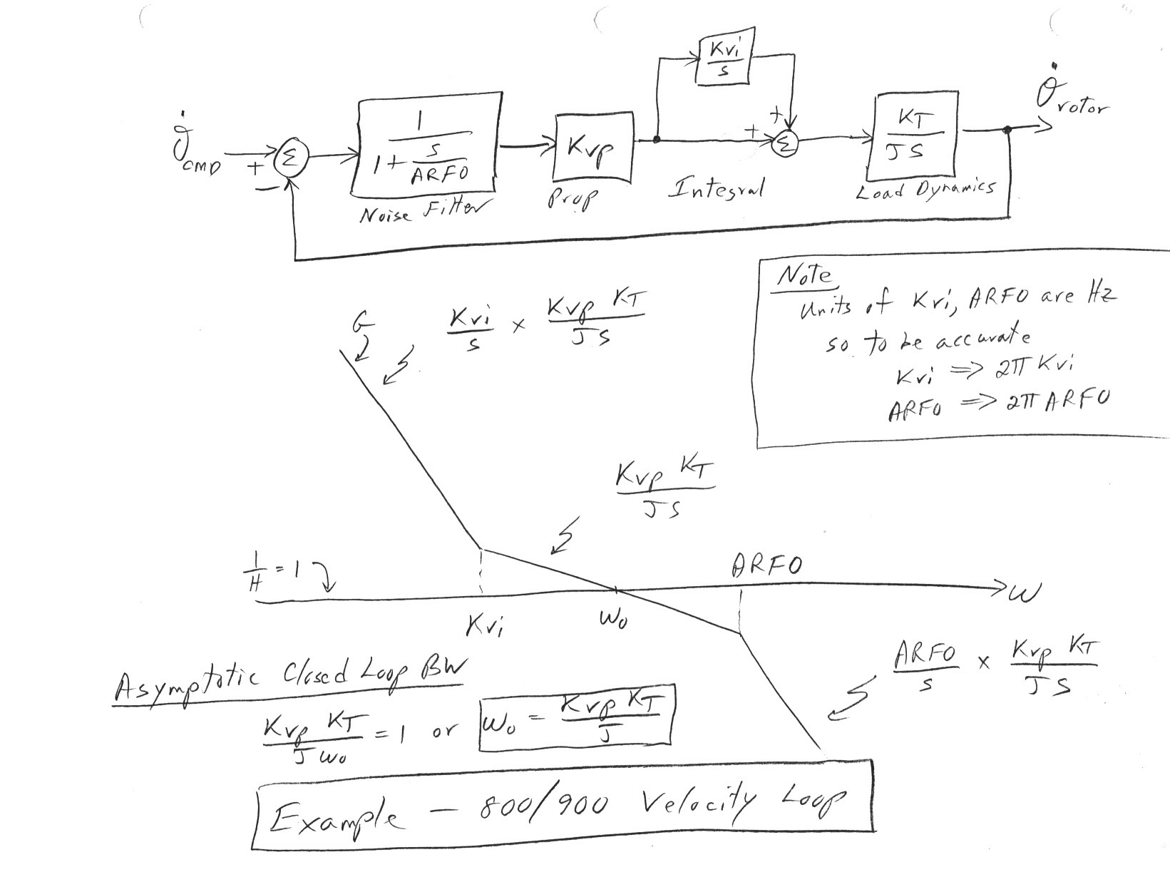
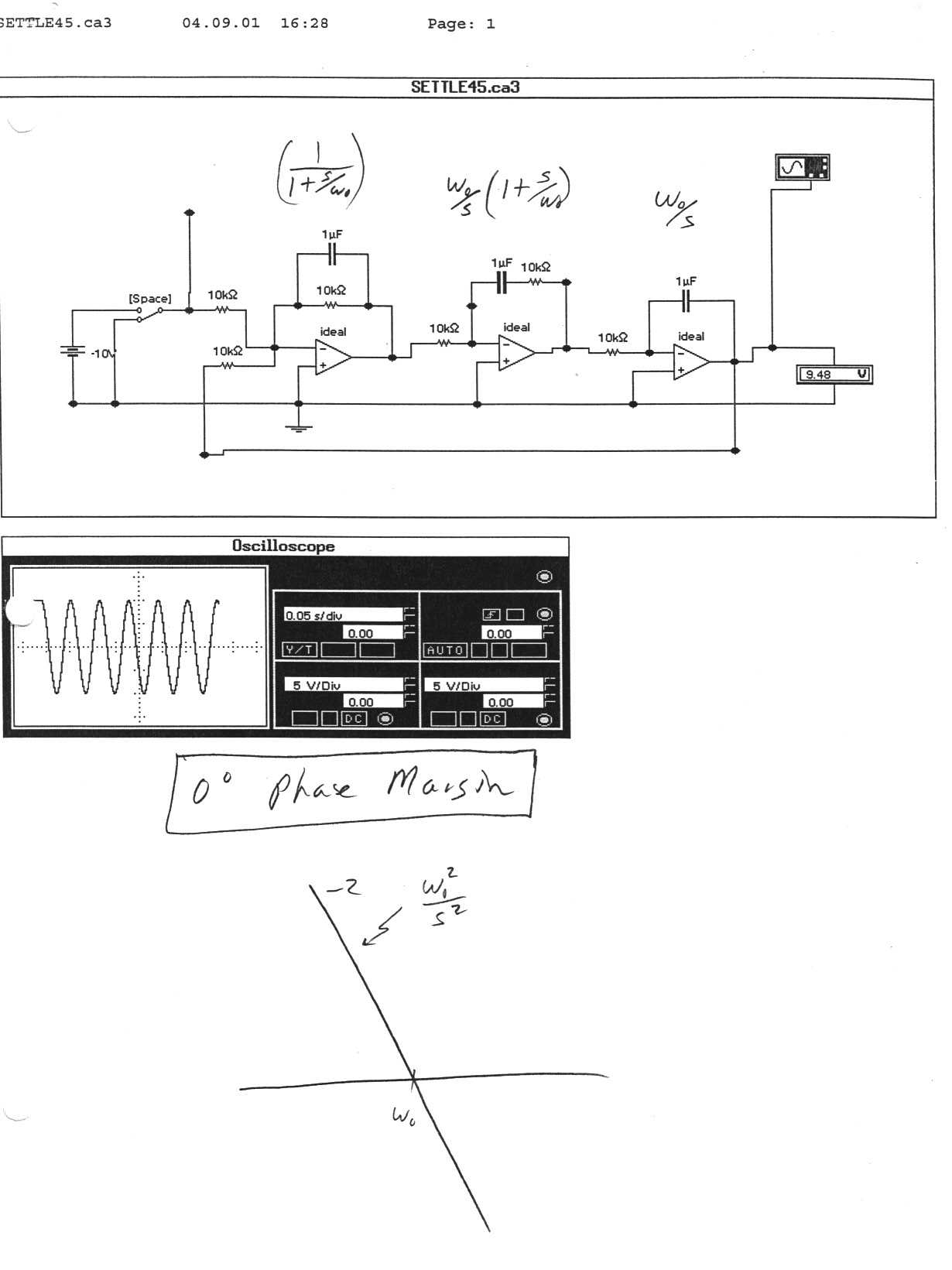
Note, '800/90 velocity loop' is just a reference to product families our company manufactured.
..
---------------------------------------------------------------------------------------------------------------------------------------------------------------------------------------------------------
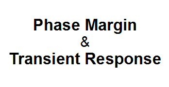
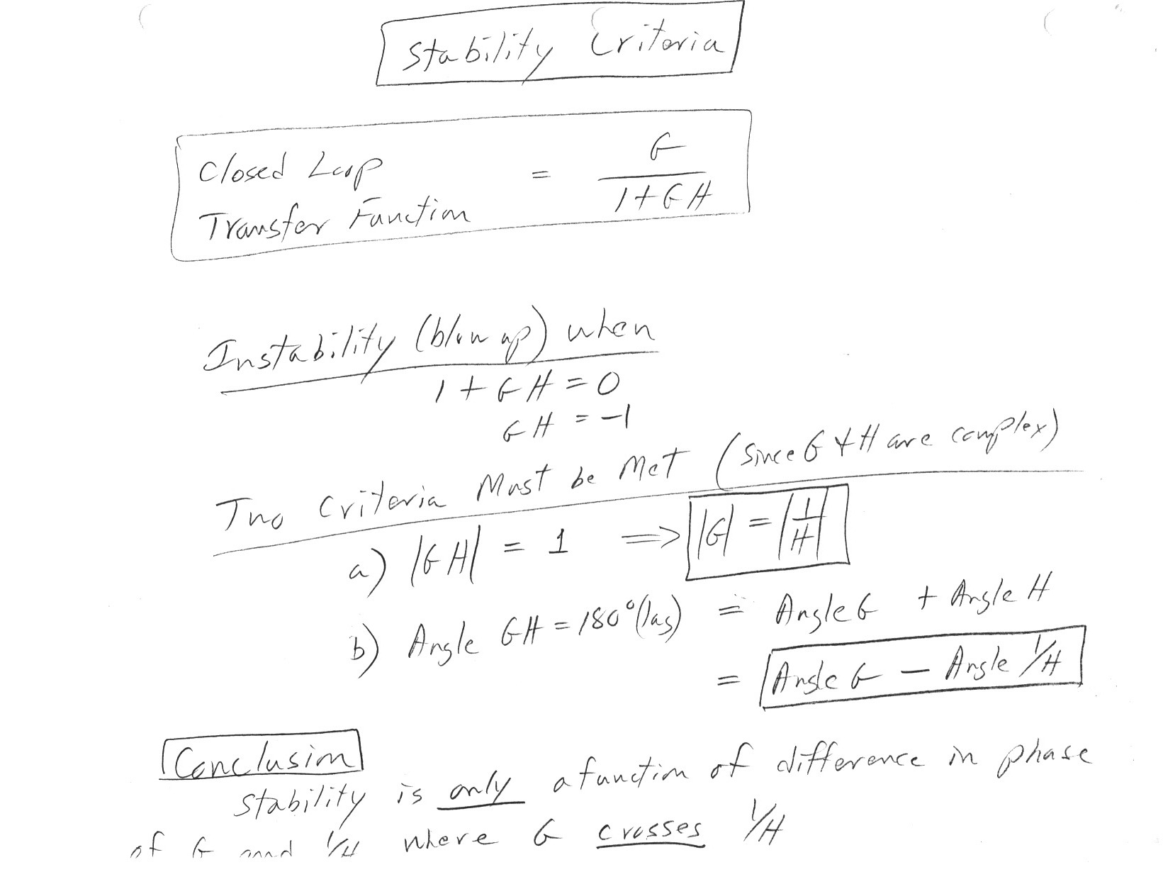
However, the denominator of a transfer function is a complex number with amplitude and phase. So for GH to equal -1, there are two criteria one based on amplitude [GH=1] and one based on phase [GH phase = 180 degrees]. [G = 1/H] is just the crossover of the straight line segments of forward and inverted feedback paths, and at this crossover frequency the phase shift around the loop, i.e. the phase shift of GH must be 180 degrees.
Phase margin---------------------------------------------------------------------------------------------------------------------------------------------------------------------------------------------------------
In modern control loop terminology a phase shift around the loop of 180 degrees at crossover means a 'phase margin' of zero degrees. Phase margin is [180 degrees minus the GH phase shift at crossover]. The degree of stability of a feedback loop is generally described in terms of its phase margin. A loop's (small signal) transient response (say to a small signal input step) can be predicted quite well from the loop's phase margin. My understanding from text books is that there is no simple exact relationship between phase margin and transient response, but relationship is close enough that in practice the the degree of of over or under shoot to a step can be predicted quite well.This makes phase margin, which as shown below can be estimated from the loop's bode diagram, a key criteria in loop design not only for stability, but also for predicting the character of the loop's transient response.
..
---------------------------------------------------------------------------------------------------------------------------------------------------------------------------------------------------------
..
Transient response vs phase margin
Below shows the
transient response from a circuit analysis program of the example control
loop circuit adjusted for various phase margins. Notice that the bode diagrams
with 45 degree and 67.5 degree phase margins have slightly different transient
response.
---------------------------------------------------------------------------------------------------------------------------------------------------------------------------------------------------------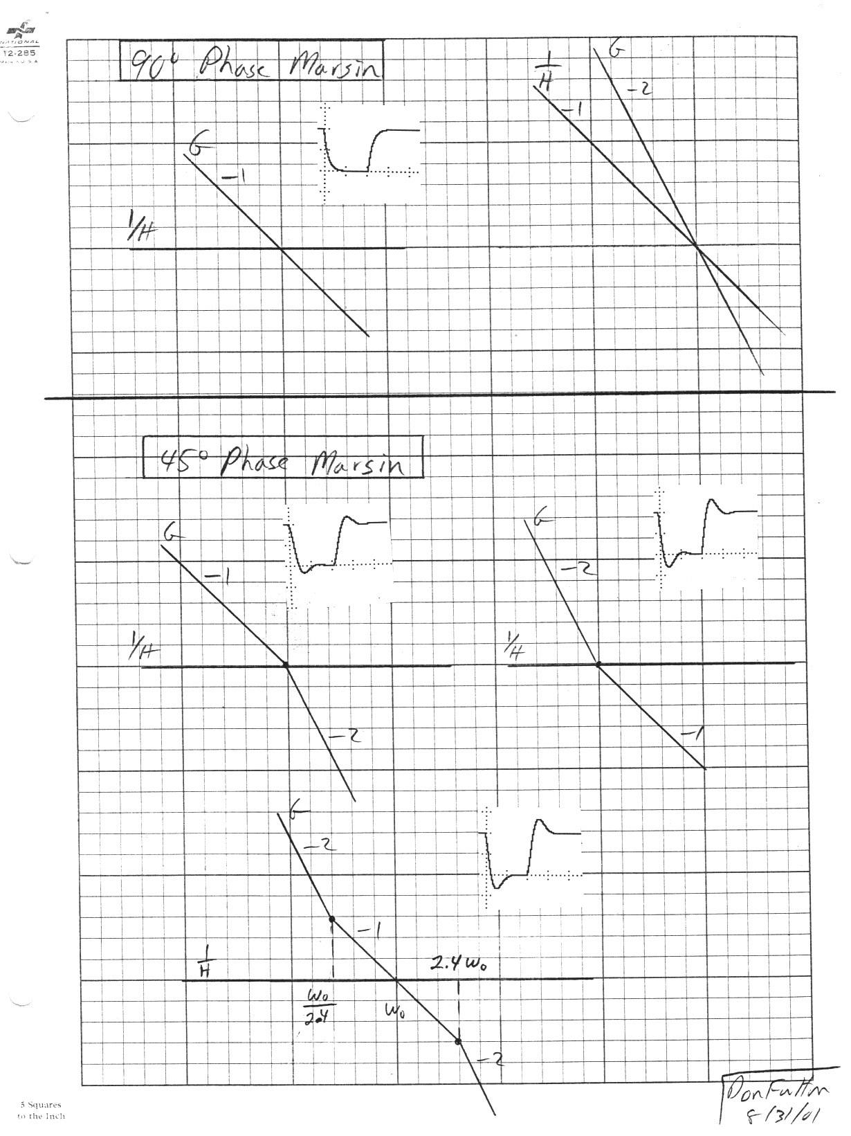
Above three systems all with 45 degree phase margin, yet with slighltly different step transient response
..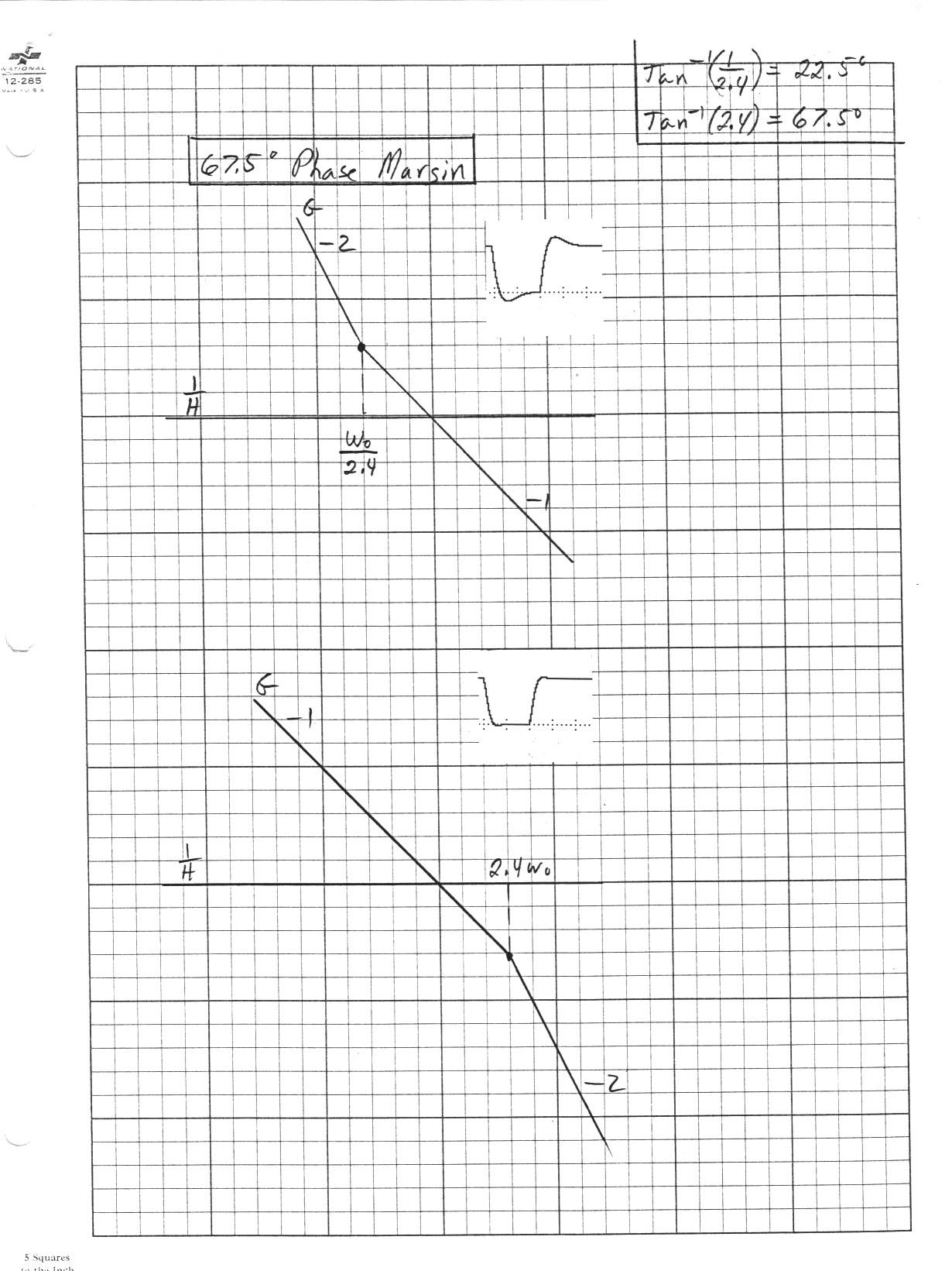
Above two systems both with 67.5 degree phase margin, yet with slighltly different step transient response
..
---------------------------------------------------------------------------------------------------------------------------------------------------------------------------------------------------------
..
..
..
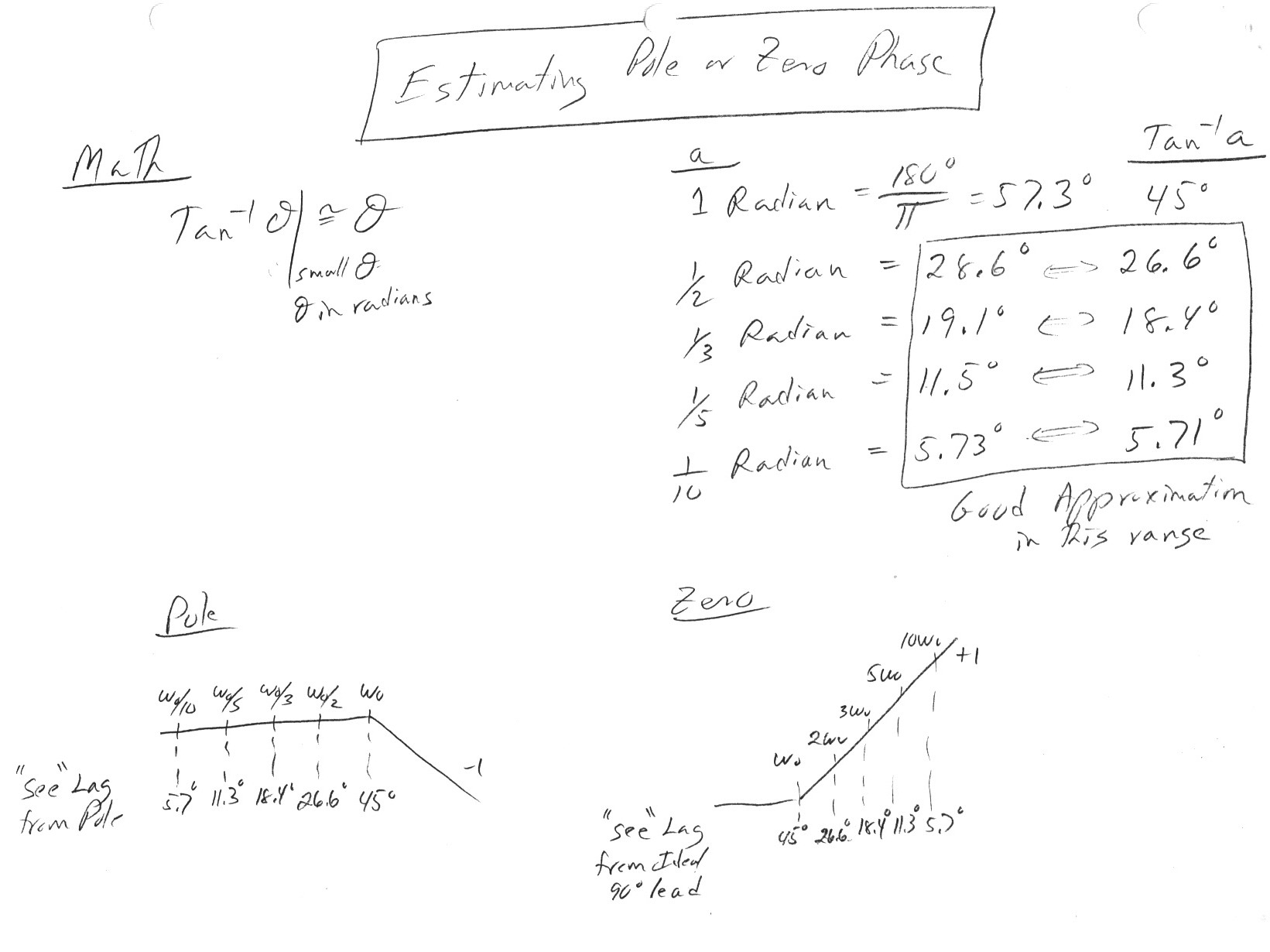
The same approximating rule also works (with a 90 degree correction) above the pole/zero. For example, a zero at 1/3rd crossover frequency contributes a phase lead at crossover of [(90 - tan^-1 (0.33)) = (90 - 18.4) = 71.6 degree].
---------------------------------------------------------------------------------------------------------------------------------------------------------------------------------------------------------
..
..
The in/out bode diagram of the closed loop just following the lower of the two curves. This is easily understood as the feedback path controls the system when the loop gain > 1, so in this frequency region the closed loop response goes as 1/H, but when the gain in the forward path gets too low such that loop gain <1, the response of the closed loop follows G.
In the circuit below, which is just simple feedback path around an integrator, the phase margin is 90 degrees since the integrator's 90 degree lag at all frequencies is subtracted from 180 degrees. From the bode diagram the 90 degree phase margin can be seen from the relative slope between the two plots which is -1 both below and above crossover regardless of the gain constant 'k'.
In the circuit below a low pass (noise filter) is added to the forward path above crossover. This will degrade phase margin because some of its lag is visible at crossover, in this case with a pole at x3 crossover a loss of 18.4 degrees since [tan-1 (1/3) = 18.4 degree]. Above 3w0 the slope difference goes from -1 to -2.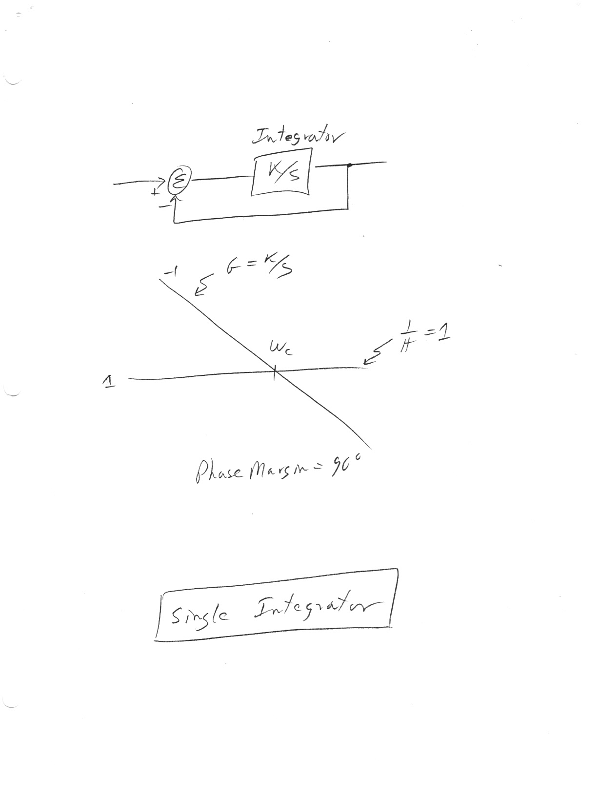
..
The circuit below with the x3 low pass above crossover moved into the feedback path has the same loss of phase margin (18.4 degree) as the circuit above, but it may not be so obvious as to why. The key here is to focus on the difference between the G and 1/H plots. This is what is really important! Above 3w0 the slope difference goes from -1 to -2, the same as the circuit above, this is why loss of phase margin is the same.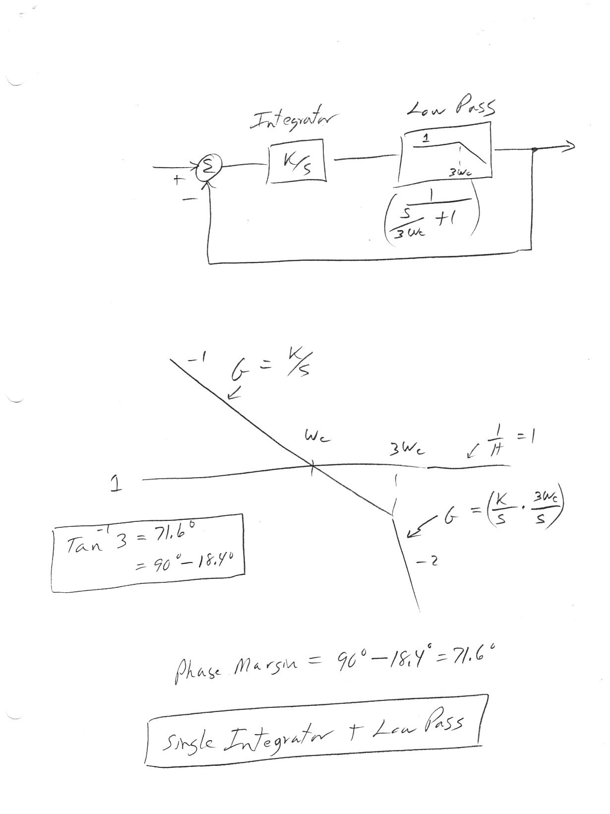
..
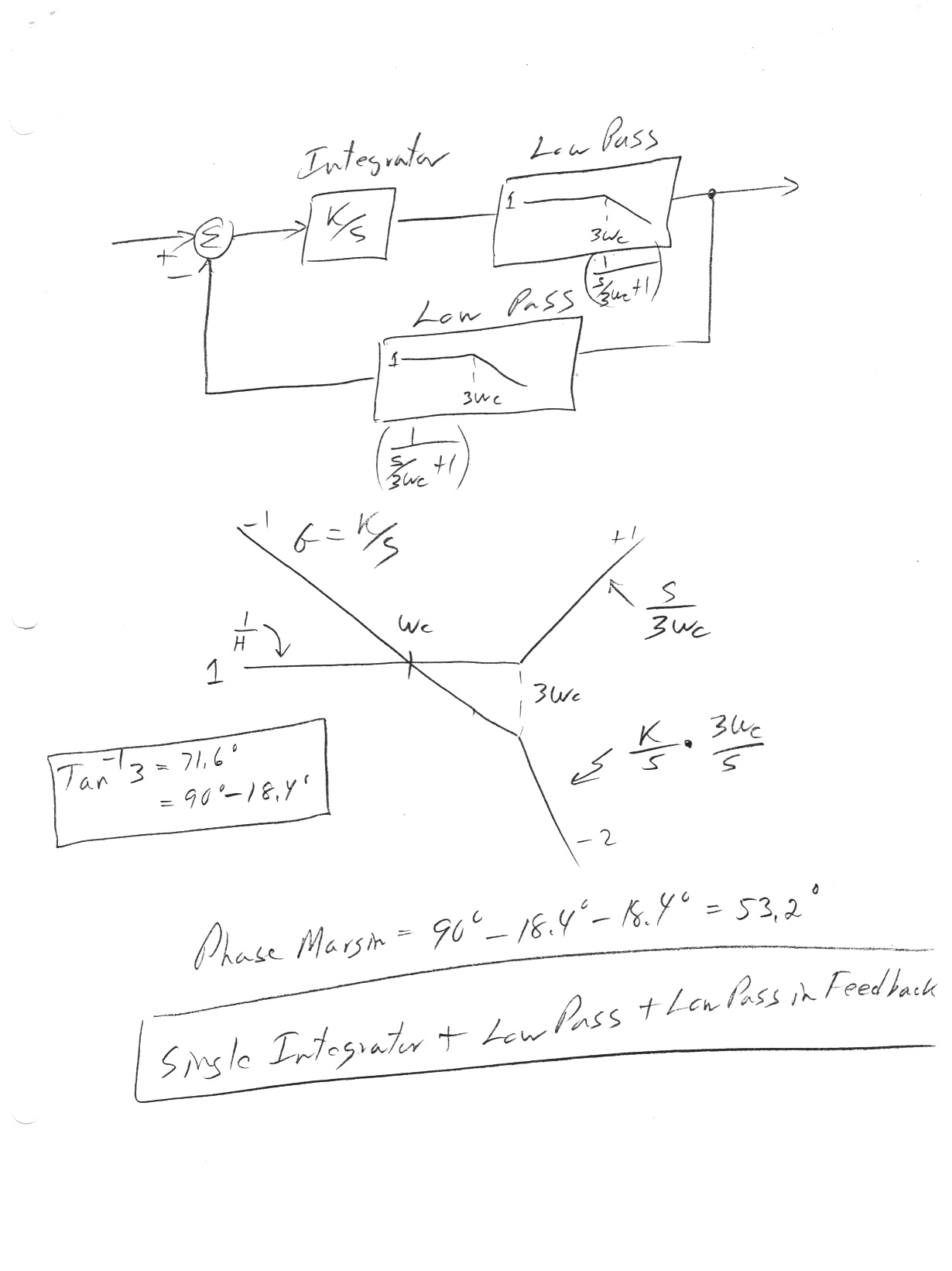
The circuit below has low pass filters at x3 above crossover in both the forward and feedback paths, so it has a bode diagram that is sort of a combination of the two circuits above. In this case above 3w0 the slope difference changes from -1 to -3, telling us that each of the low pass filters is contributing a loss of 18.4 degree in phase margin resulting in a phase margin of 53.2 degrees.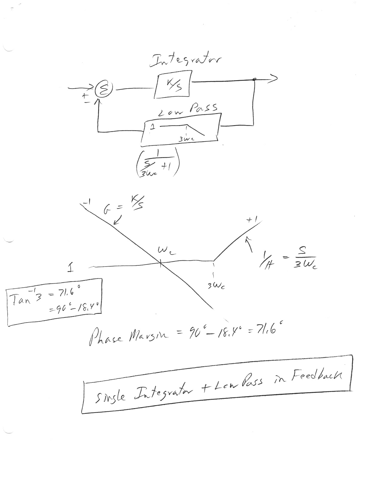
..
---------------------------------------------------------------------------------------------------------------------------------------------------------------------------------------------------------
..
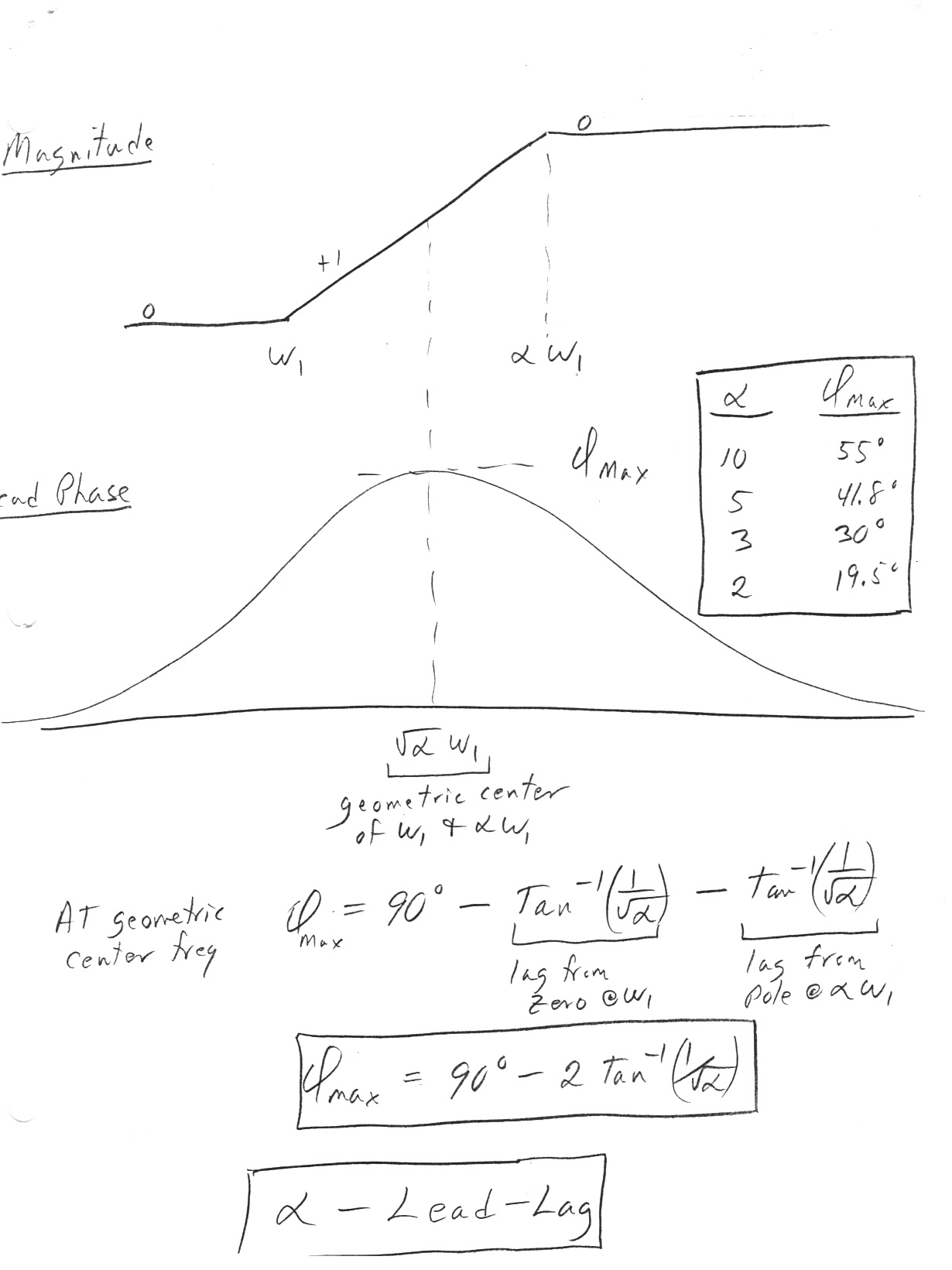
The interesting and useful feature of a lead-lag circuit for loop compensation is that its (lead) phase shift depends only on the ratio (alpha in the figure below) of its pole to zero frequency. I have tabulated its peak (lead) phase as a function of alpha in the figure below.
---------------------------------------------------------------------------------------------------------------------------------------------------------------------------------------------------------
..
---------------------------------------------------------------------------------------------------------------------------------------------------------------------------------------------------------
..
..
---------------------------------------------------------------------------------------------------------------------------------------------------------------------------------------------------------
..
..
Even now I can see in my mind the cover of this little handbook. I kept it for years even as it fell apart. However, I cannot remember the company that put it out, nor can I find any reference to it online. A google search for "bode diagram handbook" gives a null result. If I had to guess, I would say the handbook was published by Burr Brown. I remember it did have a brown cover. I've made little progress in a google search. Mostly I find histories of the early op amp companies, or the history of op amp development, or the history of integrated op amps, all of which are interesting topics that I lived through.
I remember well the excitement of well attended seminars when designers of the early integrated circuit op amps, who were well known and to some extent 'stars' in the EE world, would come to Boston (from CA or Texas) to discuss their latest circuit design tricks used in their new op amps. While commercial circuit designers like me found these new circuit tricks interesting (they were just being invented by the integrated circuit guys), they were of little practical use to us, other than to allow us to evaluate and use effectively the new op amps, because they were nearly all very specific to integrated circuits.